X-ray characterization of nanostructures
Research areas:
- Nanoscale X-ray analysis
- Nanostructured X-ray detectors
- X-ray-based spectroscopy of nanostructure devices
- In-situ X-ray studies under synthesis and fabrication conditions
Nanoscale X-ray analysis
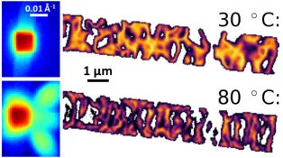
We are developing novel methods for X-ray analysis of nanostructures, in close collaboration with the MAX IV synchrotron facility. Modern X-ray optics can reach below 100 nm focus size, which allows us to probe the crystal structure, electronic properties, composition and ferroic domains with very high spatial resolution. We use X-ray diffraction (XRD), X-ray fluorescence and X-ray imaging. Coherent techniques using phase retrieval are employed to improve the spatial resolution even further. The figure shows ferroelastic domains in a single CsPbBr3 nanowire, at room temperature and above a crystal phase transition.
Contact person:
Key publication:
L.A.B. Marçal et al, In Situ Imaging of Ferroelastic Domain Dynamics in CsPbBr3Perovskite Nanowires by Nanofocused Scanning X-ray Diffraction, ACS Nano, 14(11), 15973–15982.
Nanostructured X-ray detectors
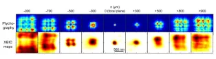
Traditional X-ray detectors use bulk crystals, which limits their resolution. We have shown that X-rays can be detected by single nanowires, with a stronger response expected. X-rays that are absorbed in a semiconductor excite electrons over the bandgap, and in the presence of an internal or external electric field the electrons will generate a measurable current. We have used this process called X-ray beam induced current (XBIC) to image the carrier collection within single nanowire solar cells at 50 nm spatial resolution. The nanowires can also be used as high-resolution X-ray detectors.
Contact person:
Key publications:
- L. Chayanun et al, Direct Three-Dimensional Imaging of an X-ray Nanofocus Using a Single 60 nm Diameter Nanowire Device, Nano Lett. 20 (11), 8326 (2020)
H Dierks et al, 3D X-ray microscopy with a CsPbBr3 nanowire scintillator, Nano Res. 16 (1), 1084 (2023)
X-ray-based spectroscopy of nanostructure devices
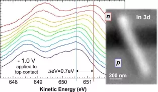
We apply X-ray photoelectron spectroscopy in order to obtain chemical information from nanostructure surfaces and interfaces and correlate it with atomic-scale structural and electronic properties. We want to know how local surface and interface composition influences device performance, therefore we study individual nanostructure devices during operation, and we follow chemical surface reactions in-situ. These experiments are performed at the MAX IV Laboratory and other synchrotron facilities.
Contact person:
Key publication:
- S. R. McKibbin et al, Operando Surface Characterization of InP Nanowire p-n Junctions, Nano Lett. 20, 887-895 (2020),
In-situ X-ray studies under synthesis and fabrication conditions
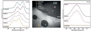
We use X-ray imaging and spectroscopy for studies of synthesis and fabrication under conditions of growth and synthesis. Modern X-ray techniques allow for studies at elevated temperatures up to at least 1000C in gaseous or liquid environments as well as under vacuum conditions. Imaging to around 100nm and studies of both structure and chemistry is possible on both on surfaces and inside complex materials. These experiments are performed at the MAX IV Laboratory and other synchrotron facilities. The example below shows the chemical composition of Indium droplets on InAs after heating up to 600C. Middle Image is of Indium metal droplets near a lithographically defined Aluminum/Paladium structure. Left and right are PhotoEmission Spectra recorded at different places in the image indicating elemental and chemical composition
Contact person:
Key publications:
- S. Benter et al. Geometric control of diffusing elements on InAs semiconductor surfaces via metal contacts. Nat Commun 14, 4541 (2023)
- L. Zhu, et al, Surface chemistry and diffusion of trace and alloying elements during in vacuum thermal deoxidation of stainless steel, Surf Interface Anal. 54(2022) 99-108